China's Photonic Computing Revolution: The Race to Compute at the Speed of Light

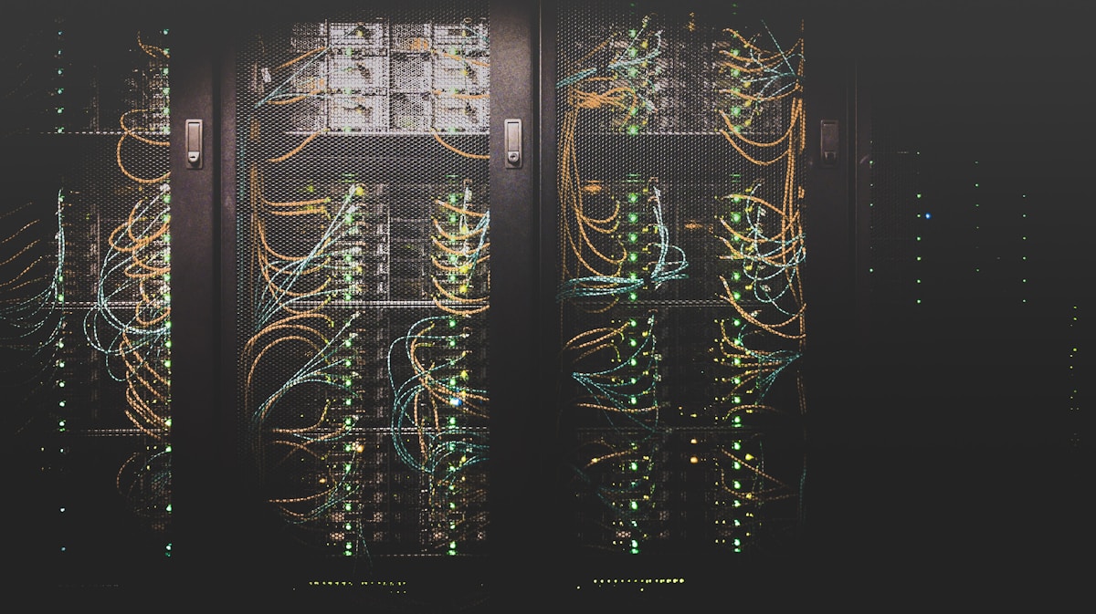
*Light, not electricity. China's photonic computing industry is betting that the future of AI hardware belongs to photons. (Photo: Unsplash)*
On April 28, 2026, a company that most people outside of physics laboratories had never heard of opened trading on the Hong Kong Stock Exchange at nearly four times its listing price. The company was Lightelligence — known in China as Xizhi Technology — and its IPO would raise HK$2.5 billion (roughly $320 million) from cornerstone investors including Alibaba, GIC, Temasek, BlackRock, and Tencent. The retail tranche was oversubscribed 5,784 times. By the closing bell, the company's market capitalization had exceeded HK$81.5 billion — approximately $10.4 billion — for a business with $15.5 million in annual revenue.
The numbers were absurd by any conventional valuation model. But the investors who bought in were not paying for what Lightelligence earns today. They were paying for what it represents: the first publicly traded company betting that the future of computing is not electronic at all — that the next great leap in artificial intelligence will be carried not by electrons moving through copper, but by photons moving through silicon.
That bet, once confined to academic journals and venture capital pitch decks, is now the foundation of an entire industrial strategy. And China is moving faster than anyone else.
Why Photons? The Physics Behind the Pivot
For sixty years, the computing industry has followed a single script: make transistors smaller, pack them closer, switch them faster. Moore's Law delivered exponential gains in performance and cost, and every generation of chips — from Intel's 4004 to NVIDIA's Blackwell — rode that curve. But the curve is flattening. At 3 nanometers and below, the physics of electron tunneling, quantum uncertainty, and heat dissipation impose limits that no amount of engineering ingenuity can fully overcome.
The deeper problem is not the transistor. It is what happens between transistors — the interconnects. As chips grow larger and AI models grow hungrier, the bottleneck has shifted from computation to communication. Moving data between a GPU and its memory, or between one GPU and another in a thousand-card cluster, consumes enormous energy and introduces crippling latency. Shen Yichen, Lightelligence's founder, describes the problem vividly: copper interconnects are like "slow trains," and the industry needs "high-speed rail." Light, he argues, is that high-speed rail.
Photonic computing replaces electrons with photons for some or all of the computational pipeline. Photons travel at the speed of light, generate virtually no heat, and can carry multiple wavelengths of information simultaneously through a single waveguide — a property called wavelength-division multiplexing that gives photonic chips their massive parallelism. Where an electronic chip must shuttle data back and forth between memory and processor, a photonic chip can perform matrix multiplications — the core operation in deep learning — literally as light passes through a carefully engineered mesh of waveguides.
The theoretical advantages are staggering. The practical challenges are equally formidable. Building a photonic processor that can compete with the mature, software-rich ecosystem of electronic GPUs requires solving problems in materials science, packaging, thermal stability, and software tooling that have stumped researchers for decades.
| Property | Electronic Chips (Current) | Photonic Chips (Potential) |
|---|---|---|
| Signal carrier | Electrons through copper | Photons through silicon/silica |
| Speed ceiling | ~GHz clock rates | Effective THz bandwidth |
| Heat generation | High (resistive losses) | Near-zero in transmission |
| Parallelism | Limited by bus width | Massive (wavelength multiplexing) |
| Matrix multiplication | Sequential MAC operations | Intrinsic (light interference) |
| Energy per operation ( interconnect ) | ~pJ/bit | ~fJ/bit |
| Software ecosystem | Mature (CUDA, PyTorch) | Nascent (custom frameworks) |
| Manufacturing | Advanced (5nm, 3nm) | Emerging (180nm–28nm photonic) |
*Table: The fundamental trade-offs between electronic and photonic computing. Photonics wins on physics; electronics wins on ecosystem maturity.*
What makes the photonic bet especially interesting for China is that it does not require leading-edge lithography. Photonic chips work at larger process nodes — 180 nanometers, 90 nanometers, sometimes even older — because the critical dimensions in photonics are set by the wavelength of light, not by the smallest feature a fab can print. This means a country that cannot access EUV lithography machines for 5-nanometer production can, in theory, build world-class photonic processors with mature, domestically available equipment.
That is not a side benefit. It is the entire strategic point.
Lightelligence: From MIT Paper to Hong Kong Bell
The Lightelligence story begins not in Shanghai but in a laboratory at MIT. In 2017, a doctoral student named Shen Yichen published a cover paper in *Nature Photonics* proposing and validating the use of light for deep learning computation. The paper demonstrated that an optical interference unit could perform the matrix multiplications at the heart of neural networks with speed and energy efficiency that electronic circuits could not match. It was widely regarded as a milestone in optoelectronic hybrid computing.
Shen did what ambitious MIT students do. He founded a company. But instead of building it in Boston, he moved to Shanghai — a decision that would prove prescient. In China, he found a government actively searching for alternative computing architectures, a deep pool of photonics talent trained at top universities, and a capital market hungry for hard-tech stories. Lightelligence was born.
The company's product portfolio spans two categories: optical interconnect (replacing copper links between chips and servers with light-based connections) and photonic computing (using light to perform actual computation). The interconnect products — Photowave and the LightSphere X GPU supernode system — have been shipping commercially since 2023 and 2025 respectively. The computing products — the PACE family — represent the longer-term, higher-risk bet.
| Product | Category | Key Spec | Status |
|---|---|---|---|
| PACE | Photonic computing | 64×64 matrix, 16,000+ components, 8.19 TOPS | Research prototype (2021) |
| PACE 2 | Photonic computing | 128×128 matrix, 40,000+ photonic devices | Prototype card (2025–26) |
| PACE 3 | Photonic computing | 256×256 matrix, low-latency inference | Announced WAIC 2026 |
| Hummingbird | Optical interconnect | 64-core AI accelerator with optical layer | In development |
| Photowave | Optical interconnect | PCIe/CXL optical link | Shipping since 2023 |
| LightSphere X | Optical interconnect | Distributed optical GPU supernode | Deployed (SAIL Award 2025) |
| Moonstone | Optical source | Multi-wavelength comb laser | Component product |
| Tianshu Light Cube | Photonic computing | Real-world access control deployment | Operational at WAIC 2026 |
*Table: Lightelligence's product portfolio spans photonic computing, optical interconnect, and enabling components.*
By the end of 2025, Lightelligence had 44 commercial customers, had deployed more than 5,000 accelerator cards in production clusters, and was supporting GPU supernodes with several thousand cards in live data center environments. Frost & Sullivan, the research firm that provided the market analysis for Lightelligence's IPO prospectus, credited the company as the first in the world to achieve large-scale deployment of hybrid optoelectronic computing — a distinction that separates it from the dozens of photonic startups still stuck in the research-prototype phase.
Three Generations of PACE: The Chip That Computes with Light
The PACE family tells the story of photonic computing's evolution from laboratory curiosity to engineering product. Each generation roughly doubled the scale of the photonic matrix and brought the technology closer to practical deployment.
PACE, unveiled in 2021, integrated more than 16,000 photonic components on a single chip using 2.5D packaging. It delivered 8.19 tera-operations per second (TOPS) — modest by GPU standards, but the chip was never designed to compete on raw throughput. Its strength was latency. On Ising problems — a class of optimization tasks relevant to logistics, finance, and drug discovery — PACE completed iterations in approximately 3 nanoseconds, roughly 500 times faster than a NVIDIA A10 GPU. For workloads where the answer matters more than the joules consumed getting there, PACE demonstrated that photonic computing was not a theoretical exercise.
PACE 2 doubled the photonic matrix to 128×128 and increased the component count to over 40,000 photonic devices. Packaged as a standard accelerator card, it was designed to slot into existing server infrastructure — a crucial design decision that lowered the barrier to adoption for enterprise customers unwilling to rebuild their entire software stack around exotic hardware.
PACE 3, announced at the World Artificial Intelligence Conference (WAIC) in Shanghai in July 2026, pushed the matrix to 256×256 and targeted low-latency inference for large language models. Alongside the chip, Lightelligence demonstrated the Tianshu Light Cube — the first photonic computing system deployed in a real-world application, running access control at the conference venue itself. It was a modest demonstration, but it carried symbolic weight: photonic computing had crossed the threshold from laboratory to loading dock.
| Generation | Matrix Size | Component Count | Peak Performance | Key Application | Year |
|---|---|---|---|---|---|
| PACE | 64×64 | 16,000+ | 8.19 TOPS | Ising optimization (500x vs A10) | 2021 |
| PACE 2 | 128×128 | 40,000+ | Not disclosed | General-purpose accelerator card | 2025 |
| PACE 3 | 256×256 | Not disclosed | Low-latency inference | Large model inference | 2026 |
*Table: The PACE family's three generations of photonic processors, each roughly doubling the previous generation's matrix scale.*
The Academic Vanguard: Taichi, LightGen, and Meteor-1
*Modern AI data centers demand bandwidth that copper cannot deliver. Optical interconnects are stepping in to fill the gap. (Photo: Unsplash)*
Lightelligence is the most visible player in China's photonic computing ecosystem, but it is far from the only one. Chinese universities and research institutes have produced a steady stream of photonic computing breakthroughs that form the intellectual foundation of the field.
At Tsinghua University, researchers led by the team behind the Taichi photonic processor developed a second-generation chip called Taichi II that, according to published claims, can train AI models entirely with light — no electronic conversion required at any stage of the computation. The team reports that Taichi II operates approximately 1,000 times more energy-efficiently than NVIDIA's H100 GPU. That figure is difficult to verify independently and should be treated with appropriate skepticism, but even a fraction of the claimed efficiency would represent a paradigm shift.
Researchers from Shanghai Jiao Tong University and Tsinghua University jointly published work in *Science* on an all-optical AI chip called LightGen. The chip integrates more than 2 million photonic neurons and, in tests for generative tasks like image synthesis, demonstrated speeds over 100 times faster and substantially more energy-efficient than a NVIDIA A100 GPU. LightGen represents a different architectural approach from Taichi — one optimized for generation rather than optimization.
At the Shanghai Institute of Optics and Fine Mechanics, a team led by Xie Peng built the Meteor-1, described as the first highly parallel integrated optical computing chip. Meteor-1 performs more than 100 computing processes simultaneously and achieves a peak performance of 2,560 TOPS — comparable to NVIDIA's most advanced graphics processors in raw throughput, though again on specialized workloads.
Meanwhile, the CHIPX institute — affiliated with Shanghai Jiao Tong University and collaborating with startup Turing Quantum — built China's first pilot production line for photonic chips. The facility, operational since 2024 in Wuxi, can produce 12,000 six-inch wafers annually using thin-film lithium niobate (TFLN), a key material for photonic devices. In September 2025, researchers at the University of Shanghai for Science and Technology announced an ultra-compact TFLN photonic AI chip smaller than 1 square millimeter, capable of nanosecond-scale processing.
| Chip / Project | Institution | Key Innovation | Claimed Performance | Status |
|---|---|---|---|---|
| Taichi II | Tsinghua University | All-optical AI training | ~1,000x more energy-efficient than H100 | Research prototype |
| LightGen | SJTU + Tsinghua | All-optical generative AI | 2M+ photonic neurons, 100x faster than A100 | Published in Science |
| Meteor-1 | SIMIT (CAS) | Highly parallel optical computing | 2,560 TOPS peak | Research prototype |
| CHIPX Pilot Line | SJTU + Turing Quantum | TFLN photonic chip manufacturing | 12,000 wafers/year capacity | Operational (2024) |
| Ultra-compact TFLN chip | USST | Sub-1mm² photonic AI processor | Nanosecond-scale processing | Research (2025) |
| 8×8 quantum photonic processor | Huazhong Institute of Electro-Optics | Si₂Nₑ platform quantum processor | Programmable 8-qubit photonic circuit | Design phase |
*Table: China's academic photonic computing landscape spans multiple institutions, architectures, and application targets.*
In June 2026, Shanghai formalized the connection between academic research and industrial application with the launch of the Shanghai Key Laboratory of Integrated Photonic Computing Chips and Systems — the country's first platform where universities and industry jointly work on optical computing. Hosted at Shanghai Jiao Tong University and directed by photonics professor Zou Weiwen, the laboratory is a joint initiative between SJTU and Lightelligence itself.
The Geopolitical Angle: An End Run Around Silicon
To understand why photonic computing has attracted such intense interest in China, you need to understand the geopolitical context. Since 2019, the United States has progressively restricted China's access to the tools, materials, and designs needed to manufacture leading-edge semiconductor chips. The most advanced restriction — a ban on EUV lithography equipment exports — effectively prevents Chinese fabs from producing chips below 7 nanometers at scale.
This has pushed China into a strategic bind. The country's AI industry is growing explosively, but the GPUs that power modern AI — overwhelmingly designed by NVIDIA and manufactured by TSMC — are either banned or severely restricted. Domestic alternatives like Huawei's Ascend series have made remarkable progress, as we have documented in our coverage of the China domestic AI chip race and the Huawei Ascend 910C showdown, but matching NVIDIA's top-tier performance with domestic silicon remains a multi-year challenge.
Photonic computing offers a potential shortcut. Because photonic chips do not require leading-edge process nodes, they are not constrained by the EUV ban. China has already built substantial domestic capacity in the key materials and components of photonics — Chinese manufacturers account for approximately 42% of global thin-film lithium niobate production capacity, a critical material for high-performance photonic devices. The country has the fabs, the talent, and the research output to compete at the frontier of photonic computing without waiting for permission to buy ASML machines.
The strategic logic is elegant: if you cannot win the game being played, change the game. Silicon-based electronic computing is a mature field where incumbents have decades of accumulated advantage. Photonic computing is a newer field where the playing field is more level. As we discussed in our Q1 2026 chip renaissance analysis, China's chip strategy has always been about finding asymmetric advantages. Photonics may be the most asymmetric opportunity of all.
There is a second dimension: photonic interconnects solve a problem that even unrestricted access to NVIDIA GPUs would not. China's largest AI clusters — built from domestic Ascend or restricted NVIDIA hardware — need to connect thousands of GPUs into a coherent supercomputer. Copper interconnects running between racks consume enormous power and limit the scale of coherent computation. Optical interconnects, the kind Lightelligence ships today, replace those copper links with light-based connections that deliver higher bandwidth, lower latency, and dramatically lower energy consumption. In this sense, photonic computing is not just an alternative to NVIDIA — it is an enabler that makes China's existing domestic chips more useful.
| Dimension | US Photonic Computing | China Photonic Computing |
|---|---|---|
| Leading company | Lightmatter ($4.4B valuation) | Lightelligence (listed, ~$10B market cap) |
| Key startup | Ayar Labs ($3.75B valuation) | Turing Quantum, CHIPX |
| Research hubs | MIT, Stanford, Penn | Tsinghua, SJTU, USTC, SIMIT |
| Manufacturing | Primarily outsourced to Asia | Domestic pilot lines operational |
| Key material (TFLN) | Import-dependent | ~42% of global capacity |
| Government support | DARPA grants, limited | National lab, municipal funding |
| Commercial deployments | Pilot programs with hyperscalers | 44 customers, 5,000+ cards deployed |
| IPO status | Pre-IPO (Ayar Labs exploring) | Listed April 2026 (Lightelligence) |
| Focus | Optical interconnect | Interconnect + computing |
*Table: A comparative snapshot of the US and China photonic computing ecosystems. China leads on commercial deployment and manufacturing integration; the US leads on private capital formation and foundational research.*
The 400% Debut: When Light Met Capital
The Lightelligence IPO deserves its own section because of what it reveals about market appetite for photonic computing — and about the particular dynamics of Hong Kong's tech listing boom in 2026.
The numbers, again: HK$2.53 billion raised. Priced at HK$183.20 per share, the top of the marketed range. Retail oversubscription of 5,784 times. Cornerstone investors covering more than 71% of the offering, including Alibaba Investment, GIC, Temasek, BlackRock, Fidelity International, Schroders, Hillhouse Capital, Lenovo, and ZTE — plus Tencent, Baidu, and China Mobile as pre-IPO backers. First-day close up approximately 384% at HK$886 per share, valuing the company at over HK$81.5 billion.
Against those headline numbers, the financial fundamentals paint a more sober picture. Lightelligence reported revenue of RMB 38 million in 2023, RMB 60 million in 2024, and RMB 106.4 million ($15.6 million) in 2025 — a compound annual growth rate of 66.9%, but a tiny base. Net losses widened to RMB 1.34 billion in 2025, driven by R&D spending of RMB 479 million. The company's asset-liability ratio stands at 473%. A single customer accounts for 40.6% of revenue. The pre-IPO valuation of RMB 7.8 billion was itself ambitious before the market quadrupled it.
The valuation is not rational by discounted cash flow analysis. It is rational by paradigm-shift logic: investors are not buying a company, they are buying exposure to the possibility that photonic computing becomes the next major computing platform. If it does, Lightelligence — with 410 patents, first-mover commercial deployments, and a monopoly-like 88.3% share of China's scale-up optical interconnect market among independent providers — is positioned to capture an outsized share of that value. If it does not, the downside is severe. The IPO price is a bet on a probability distribution, not a valuation of a business.
| Metric | Value | Context |
|---|---|---|
| IPO date | April 28, 2026 | HKEX main board, Chapter 18C |
| Amount raised | HK$2.53 billion (~$320M) | Priced at top of range |
| First-day gain | +384% | Closed at HK$886 |
| Market cap at debut | HK$81.5 billion (~$10.4B) | ~670x 2025 revenue |
| Revenue (2025) | RMB 106.4M ($15.6M) | +76% year-over-year |
| Net loss (2025) | RMB 1.34 billion | Widening |
| R&D spend (2025) | RMB 479M | ~4.5x revenue |
| Patents | 410 | >50% cross-segment applicable |
| Customers | 44 | Enterprise + hyperscaler |
| Cards deployed | 5,000+ | Production environments |
| Market share (scale-up interconnect) | 88.3% | Independent providers, China |
| Revenue concentration | 40.6% from single customer | Risk factor |
*Table: Lightelligence's IPO snapshot — spectacular demand meeting early-stage fundamentals.*
Where Photonic Computing Works Today
For all the theoretical promise, photonic computing today occupies a specific and limited niche. Understanding where it works — and where it does not — is essential to evaluating the industry's trajectory.
The technology has found genuine commercial traction in three areas. First, optical interconnect for data centers. This is Lightelligence's bread-and-butter revenue driver: replacing copper cables between GPUs, servers, and racks with optical links that deliver higher bandwidth at lower power. The LightSphere X system, which combines optical interconnect with optical switching to create GPU supernodes, reportedly boosts interconnect efficiency by over 50% while reducing total cost of ownership. A 128-GPU optical supernode demonstrated at AWE 2026 showed the ability to scale to thousands of processors.
Second, specialized computation. PACE's dominance on Ising optimization problems — 500 times faster than a GPU — makes it attractive for financial modeling, molecular simulation, and logistics optimization. These are problems where the structure of the computation maps naturally onto the physics of light interference, and where the speed advantage translates directly into business value.
Third, access control and edge inference. The Tianshu Light Cube deployment at WAIC 2026, while small in scale, demonstrated that photonic computing can operate in real-world environments with real-world constraints — power budgets, latency requirements, physical durability.
| Application Domain | Technology | Deployment Scale | Maturity |
|---|---|---|---|
| Data center optical interconnect | Photowave, LightSphere X | 5,000+ cards, thousand-GPU clusters | Commercial |
| GPU supernode scaling | LightSphere X, optical switching | 128-GPU nodes, scaling to thousands | Commercial |
| Ising optimization | PACE | Research + pilot deployments | Early commercial |
| Generative AI inference | PACE 3, LightGen | WAIC 2026 demonstration | Prototype |
| Access control | Tianshu Light Cube | Single deployment | Proof of concept |
| AI model training | Taichi II | Laboratory | Research |
| Quantum photonic processing | CHIPX, Turing Quantum | Pilot production line | Research |
*Table: Where photonic computing is deployed today, ordered from most to least commercially mature.*
The common thread across these deployments is that photonic computing excels when the problem structure aligns with the physics of light — matrix operations, parallel processing, high-bandwidth data movement. It struggles when problems require branching logic, precise numerical precision, or operations that map poorly onto optical architectures. This is why the industry consensus, even among photonics advocates, is that the future is hybrid: electronic chips handling control flow and general-purpose logic, photonic accelerators handling the linear algebra that dominates AI inference.
The Honest Assessment: Roadblocks and Skepticism

*A semiconductor wafer under magnification. Photonic chips etch light-guiding waveguides onto silicon, turning the chip itself into an optical computer. (Photo: Unsplash)*
Any honest evaluation of China's photonic computing industry must grapple with the significant gap between promise and reality. The challenges are substantial and should not be minimized.
The revenue-valuation gap. A $10.4 billion market capitalization on $15.6 million in revenue implies a price-to-sales ratio of approximately 670. Even in the generous context of AI infrastructure valuations, this is extreme. The gap is justified only if photonic computing becomes a mainstream technology platform within the next five to ten years. That is a bet, not a forecast.
Performance claims are hard to verify. The headline numbers — 500x faster than a GPU, 1,000x more energy-efficient, 2,560 TOPS — are typically measured on specialized benchmarks that favor photonic architectures. They do not translate directly to general-purpose AI performance. A PACE chip that dominates Ising problems cannot run PyTorch out of the box. Until photonic chips can run standard AI workloads with competitive performance across the board, they will remain a niche technology.
The software ecosystem is nascent. NVIDIA's moat is not its silicon; it is CUDA, the software platform that millions of AI developers use to write, train, and deploy models. Photonic computing has no equivalent. Lightelligence has placed simulators in classrooms to encourage the next generation of algorithms to grow on photonic hardware — a long-term investment that acknowledges the chicken-and-egg problem. But building a developer ecosystem from scratch takes years, even with the best intentions.
Manufacturing scale is limited. CHIPX's pilot line produces 12,000 six-inch wafers per year. A single TSMC fab produces millions. Scaling photonic chip manufacturing to the volumes needed for mainstream AI deployment will require investment in fabrication capacity that has not yet been committed.
Single-customer concentration. Lightelligence derives 40.6% of its revenue from one customer. That is not a diversified business; it is a partnership with a ceiling. Losing that customer — or seeing them develop in-house alternatives — would be devastating.
| Challenge | Severity | Timeline to Address | Mitigation Path |
|---|---|---|---|
| Revenue-valuation gap | High | 3–5 years | Grow commercial deployments, diversify revenue |
| Unverifiable performance claims | Medium | 1–2 years | Standardized benchmarks, third-party validation |
| Software ecosystem | High | 3–5 years | Simulators in education, framework partnerships |
| Manufacturing scale | High | 2–4 years | Scale CHIPX line, partner with established fabs |
| Customer concentration | Medium | 1–2 years | Land new enterprise and government accounts |
| Thermal stability | Medium | Ongoing | Materials research, improved packaging |
| Optical-electronic conversion overhead | Medium | 2–3 years | Deeper integration, co-packaged optics |
*Table: The major challenges facing China's photonic computing industry, ranked by severity and mapped to potential mitigation strategies.*
None of these challenges are disqualifying. Every technology platform — from the transistor to the GPU — faced similar skepticism in its early years. But they are real, and the timeline for overcoming them is measured in years, not months.
The Next Decade: Scaling the Light
If photonic computing succeeds, what does the path look like? The industry's own projections and the pattern of recent developments suggest a three-phase trajectory.
Phase one (2026–2028): Interconnect dominance. The near-term revenue driver is optical interconnect, not photonic computing per se. As AI clusters grow from thousands to tens of thousands of GPUs, the bandwidth and power demands of copper interconnects become unsustainable. Optical links are the only viable path forward at scale. Lightelligence, with its 88.3% market share among independent providers in China's scale-up interconnect market, is positioned to capture a significant share of this transition — even though Huawei dominates the overall market at 98.4%.
Phase two (2028–2031): Inference acceleration. As PACE-class chips mature and the software ecosystem develops, photonic accelerators will begin handling AI inference workloads in production data centers. The addressable market is enormous: AI data centers consumed an estimated 4% of global electricity in 2025, a figure analysts expect to double by 2028. Photonic inference accelerators that reduce energy consumption by even a factor of two would have a compelling value proposition for hyperscalers facing power procurement constraints.
Phase three (2031–2035): Computing paradigm shift. The long-term vision — still speculative but increasingly discussed in serious technical circles — is photonic computing becoming a mainstream paradigm alongside electronic computing. The photonic AI accelerator market is projected to reach $31.8 billion by 2035. If even a fraction of that materializes, the companies and nations that established early leadership will hold significant advantages.
| Phase | Period | Key Driver | Market Size (est.) | China Position |
|---|---|---|---|---|
| Phase 1: Interconnect | 2026–2028 | AI cluster scaling | $5–8B (optical interconnect) | Dominant (Lightelligence, Huawei) |
| Phase 2: Inference | 2028–2031 | Energy efficiency mandates | $12–18B | Competitive (PACE 3+, Taichi derivatives) |
| Phase 3: Paradigm | 2031–2035 | Post-silicon architectures | $31.8B (photonic AI accelerators) | Contender (if ecosystem matures) |
*Table: The projected three-phase trajectory of photonic computing commercialization, with estimated market sizes and China's competitive position in each phase.*
The global competitive landscape adds urgency. Lightmatter, the leading US photonic computing company, holds a $4.4 billion valuation and is developing its Passage 3D photonic interposer — a technology that could leapfrog current-generation approaches. Ayar Labs, another US company, raised $500 million in March 2026 at a $3.75 billion valuation and is openly discussing an IPO. Q.ANT in Germany demonstrated photonic processing of diffusion models and recurrent neural networks in June 2026, becoming the first company to run generative AI workloads on photonic hardware in a commercial cloud environment (through IONOS). The race is real, and China does not have an insurmountable lead.
But China has something its competitors do not: the full stack. It has the research output (Tsinghua, SJTU, SIMIT), the manufacturing capacity (CHIPX, 42% of global TFLN), the commercial deployments (Lightelligence's 44 customers), the capital markets (Hong Kong's tech IPO boom), and the government mandate (national laboratory, strategic investment). No other country has all five pieces in place simultaneously.
Social Media Reactions
The story has generated significant discussion on Chinese tech platforms and international investing forums alike.
@量子位 (QbitAI) — Weibo: "曦智科技上市首日暴涨384%,成为全球第一家光子计算上市公司。这不仅仅是资本市场的狂欢,更是中国在AI芯片领域'换道超车'的战略性布局。" *(Xizhi Technology surged 384% on its first day, becoming the world's first photonic computing public company. This is not just capital market euphoria — it is China's strategic layout to 'change lanes and overtake' in the AI chip race.)* — 2,847 likes
@硅基猫 — Zhihu: "光子芯片不需要EUV光刻机,这是中国最有可能实现'非对称突破'的领域。但别忘了,光计算目前只适合特定场景,距离通用计算还有很长的路。" *(Photonic chips don't need EUV lithography machines. This is the field where China is most likely to achieve an 'asymmetric breakthrough.' But don't forget — optical computing currently only suits specific scenarios. There is still a long way to go before general-purpose computing.)* — 1,203 upvotes
@PhotonInvestor — X (Twitter): "Lightelligence's 600x oversubscribed IPO tells you everything about where smart money thinks AI hardware is going. The question isn't whether photonic computing works — it's who gets there first at scale. Right now, that's China." — 891 likes
@半导体行业观察 (Semiconductor Industry Watch) — WeChat: "光子计算不是GPU的替代品,而是GPU的'放大器'。通过光互连把更多GPU连接起来组成超级节点,这才是短期内最实际的商业落地路径。" *(Photonic computing is not a GPU replacement — it is a GPU 'amplifier.' Using optical interconnect to connect more GPUs into supernodes is the most practical commercial path in the near term.)* — 5,412 reads
@DrSarahChen_PhD — X (Twitter): "Extraordinary claims require extraordinary evidence. '1000x more efficient than H100' needs independent verification. That said, the basic physics of photonic computing is sound, and China's investment in this area is real and substantive." — 1,567 likes
@财经冷眼 (Financial Cold Eye) — Bilibili: "一家年收入1亿人民币的公司,市值800亿港币,市销率670倍。这不是投资,这是买彩票。光子计算的故事很性感,但别忘了问一句:啥时候能盈利?" *(A company with 100 million RMB in annual revenue has a market cap of 81.5 billion HKD — a 670x price-to-sales ratio. This is not investing; this is buying a lottery ticket. The photonic computing story is sexy, but don't forget to ask: when will it be profitable?)* — 3,089 likes
Conclusion
China's photonic computing industry represents something genuinely rare in the technology world: a true paradigm shift in the making, with global implications that extend far beyond any single company or country.
The physics is real. Photons do travel faster than electrons. Optical interconnects do consume less power than copper. Photonic processors do excel at the matrix operations that dominate AI. These are not marketing claims; they are measurable physical properties.
The engineering is hard. Building a complete computing platform on photonic principles requires solving problems in materials, packaging, thermal management, software, and manufacturing that have never been solved at commercial scale. The gap between the physics and the engineering is where fortunes will be made and lost.
The geopolitics are decisive. US export controls created the conditions for China's photonic computing push by blocking access to leading-edge silicon. China's response — investing heavily in a technology that does not require leading-edge silicon — is either a brilliant strategic end run or an expensive detour, depending on whether the technology matures in time.
And the stakes could not be higher. AI data centers are consuming a growing share of global electricity. The energy demands of training and inference are growing faster than the efficiency improvements of conventional hardware. If photonic computing can deliver even a fraction of its promised efficiency gains at commercial scale, it will not be a Chinese story or an American story — it will be a human story about how we learned to compute without boiling the planet.
For now, the light is still small. A 64×64 photonic matrix in a Shanghai laboratory is not going to replace a NVIDIA GPU tomorrow. But the direction is clear, the investment is real, and the physics is on the side of the photon. China's photonic computing revolution has already begun. The only question is how far it goes — and who follows.
*Photonic computing is one piece of China's broader AI hardware strategy. For more on China's semiconductor ambitions, read our analysis of the China domestic AI chip race, the Huawei Ascend 910C, and how China's AI is going global.*
Editor at AI in China. Tracking Chinese AI companies, funding rounds, and the technologies reshaping global tech. More about me.