4096 Chips, One Machine: Inside Huawei's Ascend 960 SuperNode and the World's First 3D AI Data Center
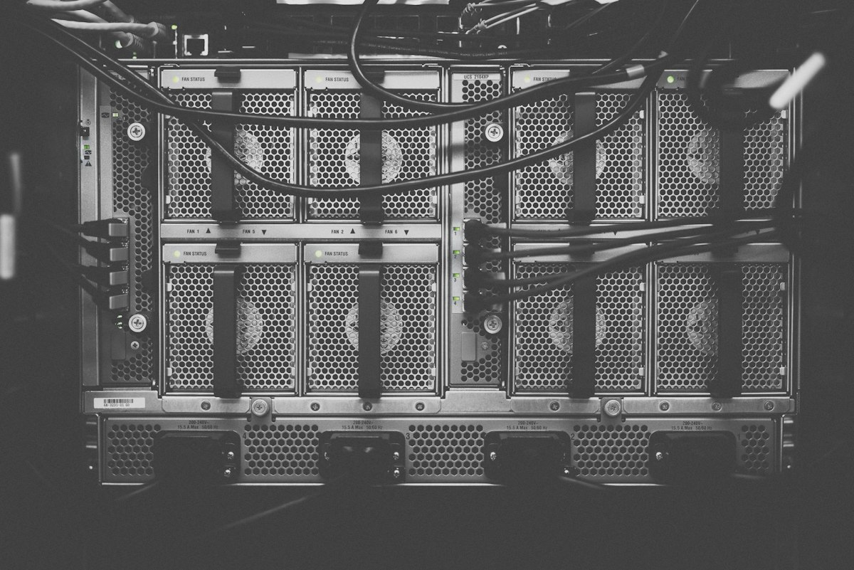
*Photo: The Ascend 960 SuperNode compresses what would have been an entire data center hall into a single machine the size of a shipping container. Image: Unsplash*
The Photonics Gambit
At 2:47 PM on September 17, 2026, Wang Tao — Huawei's deputy chairman and rotating CEO — held a small rectangular module above his head on the keynote stage of Huawei Connect in Shanghai. To the 20,000 people in the audience, it looked unremarkable: a slab of metal and glass about the size of a smartphone. But the module, called Hi-ONE, represented something that no semiconductor company on Earth had yet shipped at scale: a near-packaged optics engine that moves data between AI chips at the speed of light without leaving the circuit board.
That module is the connective tissue of the Ascend 960 SuperNode, the machine Wang unveiled minutes later. One supernode contains 4,096 Ascend 960 AI accelerators, delivers 8 exaflops of FP8 compute, houses 1 petabyte of high-bandwidth memory, and replaces 48,000 conventional 800G optical modules with just 5,500 Hi-ONE units — cutting power consumption by more than 550 kilowatts and doubling mean-time-between-failures. In a single rack-scale system, Huawei has built what a traditional data center would need an entire hall to house.
Twenty-four hours earlier, 340 kilometers west in Wuhu, Anhui Province, a different kind of first was taking place. The doors of what Huawei calls the world's first 3D data center swung open to industry delegates at the AIDC Industry Development Conference. Rather than sprawling horizontally across a campus, this facility stacks cooling, compute, power, and backup layers vertically — a silicon skyscraper where the IT floor hosts 1,024-card Ascend 950 supernodes and the building's total compute capacity reaches 100,000 cards, all cooled by water drawn from the adjacent Yangtze River.
Two announcements. Two cities. One message: China is no longer playing catch-up in AI infrastructure. It is writing new rules.
From Blockade to Breakthrough
To understand why these announcements matter, you need to rewind to 2019, when the United States placed Huawei on its Entity List, cutting off access to advanced semiconductors and the tools to manufacture them. The conventional wisdom at the time was that Huawei — and by extension, China's AI ambitions — would be kneecapped. Without TSMC's leading-edge fabs and Nvidia's GPUs, how could China possibly compete?
Huawei's answer, refined over seven years of sanctions, has been to stop competing on Moore's Law's terms entirely. Instead of chasing smaller transistors — a race blocked by restrictions on EUV lithography — Huawei has pursued what its semiconductor chief He Tingbo calls the Tau (τ) Scaling Law: rather than shrinking geometry, compress time. The idea, first systematized in a paper He published on ChinaXiv in May 2026, is that the industry's future belongs to whoever can most effectively reduce signal propagation delay across the entire system — from individual transistors to interconnects to packaging to cluster topology.
Over the past six years, Huawei has designed and mass-produced 381 chips based on τ-law principles. The Kirin 2026 smartphone chip, launching this fall, is the first product to use LogicFolding — stacking digital, analog, and memory circuits vertically to boost transistor density from 155 million to 238 million transistors per square millimeter in a single generation, a jump that would have taken three cycles under traditional geometric scaling. But the τ-law's most dramatic expression is not in phones. It is in the data center, where He Tingbo's team calculated that more than 80% of energy is consumed not by computation itself but by moving data between chips.
That insight — that data movement, not computation, is the true bottleneck — is the intellectual foundation of both the Ascend 960 SuperNode and the 3D data center. It is also, not coincidentally, the same insight driving Nvidia's own roadmap. But Huawei, constrained by manufacturing limits that Nvidia does not face, has been forced to pursue system-level efficiency far more aggressively.
Anatomy of a SuperNode
The Ascend 960 SuperNode is the third generation of Huawei's supernode architecture, following the 384-card and 910C-based 4,096-card systems that preceded it. What distinguishes the 960 is not just scale but the integration of near-packaged optics — technology that Nvidia has discussed publicly but has not yet shipped in a commercial product.
Traditional AI clusters connect chips using copper cables for short distances and pluggable optical transceivers for longer runs. Both approaches waste enormous amounts of power and space. Each 800G optical module consumes 13 to 15 watts and occupies a physical slot. In a cluster of 100,000 chips, you need tens of thousands of these modules, each a potential failure point.
NPO moves the optical engine directly onto the compute board, adjacent to the chip package. This eliminates the retimer chips, reduces signal loss, and slashes power consumption. The numbers are stark:
| Metric | Traditional 800G Optics | Hi-ONE NPO | Improvement |
|---|---|---|---|
| Modules needed (4,096-card supernode) | ~48,000 | 5,500 | 88.5% fewer |
| Power per module | 13–15 W | ~5 W (integrated) | ~65% lower |
| Total interconnect power (supernode) | ~720 kW | ~165 kW | >550 kW saved |
| Signal reach | Rack-level (copper) | 100m+ (optical) | Cross-facility |
| Mean time between failures | Baseline | 2x baseline | 2x improvement |
| Single-module bandwidth | 800 Gb/s | 7.2 Tb/s | 9x increase |
*Table 1: Hi-ONE near-packaged optics versus traditional pluggable optical modules in supernode deployment. Sources: Huawei Connect 2026 keynote, OIF technical presentations.*
Huawei proposed the NPO standard at the Optical Internetworking Forum (OIF) and is currently the only company mass-producing NPO modules with built-in light sources. The Hi-ONE engine delivers 7.2 terabits per second per module — nine times the bandwidth of a conventional 800G module — and is designed to pair with what Huawei calls the Unified Bus, a system interconnect that reduces remote memory access latency from tens of microseconds to approximately 100 nanoseconds, a 500-fold improvement.
Inside a single Ascend 960 SuperNode:
| Specification | Ascend 960 SuperNode |
|---|---|
| AI accelerators | 4,096 Ascend 960 chips |
| FP8 compute | 8 EFLOPS |
| FP4 compute | 16 EFLOPS |
| High-bandwidth memory | 1 PB |
| HBM bandwidth (per card) | 9.6 TB/s |
| Memory capacity (per card) | 288 GB |
| Interconnect | Hi-ONE NPO + Unified Bus |
| Cluster availability | 99.8% |
| Networking topology | 2-layer CLOS, 4-plane |
*Table 2: Ascend 960 SuperNode headline specifications as announced at Huawei Connect 2026.*
Individual Ascend 960DT cards deliver 2 petaflops of FP8 compute and 4 petaflops of FP4, with 288 GB of HBM — specifications that are competitive with, though not superior to, Nvidia's B300 on raw silicon metrics. But Huawei's argument has never been about single-chip superiority. It is about what happens when you stop thinking in terms of chips and start thinking in terms of systems.
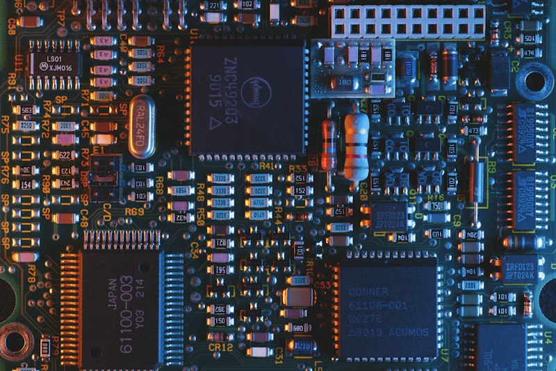
*Photo: Near-packaged optics engines like Huawei's Hi-ONE sit directly on the compute board, eliminating the power-hungry pluggable transceivers that traditional AI clusters require by the tens of thousands. Image: Unsplash*
The Machine That Folded the Data Center
The Wuhu 3D data center, which opened to industry visitors on September 16, is the architectural counterpart to the supernode. Just as the supernode folds chips into a unified system, the 3D data center folds an entire facility into a vertical stack.
Traditional data centers are built like suburban office parks: long, low buildings spread across hectares of land, with cooling systems, server halls, and power infrastructure arranged horizontally. Construction is slow and bespoke — every facility is effectively a unique construction project with 12-to-18-month build times. The Wuhu facility inverts this entirely.
| Layer | Function | Key Details |
|---|---|---|
| Layer 4 (Top) | Backup power | Independent backup systems, isolated from IT floors |
| Layer 3 | Power supply | Dedicated power distribution with zone-level redundancy |
| Layer 2 | IT equipment | 1,024-card Ascend 950 supernodes, 100K-card total capacity |
| Layer 1 (Base) | Cooling | Natural Yangtze River water source, decoupled from IT layer |
*Table 3: Wuhu 3D data center layer architecture. Each layer is physically isolated to prevent fault propagation between systems.*
The benefits are quantifiable. By shifting from "construction site building" to "factory prefabrication, on-site assembly," mechanical and electrical delivery timelines are cut in half. The vertical design enables zone isolation — a fault in one layer does not cascade to others. And by using the Yangtze River as a natural cooling source, the facility dramatically reduces dependence on energy-hungry chillers.
Huawei has published a book on 3D data center design and released an open design library, signaling that it intends this architecture to become an industry standard — and that it wants to be the company defining that standard. In a world where AI compute demand is doubling roughly every six months, the ability to build data centers twice as fast is not a marginal improvement. It is a structural advantage.
The Deployment Map
Hardware announcements are only as credible as the deployments behind them. Here, the evidence is mounting rapidly.
The most significant signal came on September 4, when Bloomberg reported that DeepSeek plans to deploy at least 160,000 Ascend 950DT chips at a gigawatt-scale data center in Ulanqab, Inner Mongolia — exclusively for inference. At an estimated street price of roughly $16,000 per chip (though prices have reportedly risen to about 250,000 yuan, or $35,000, amid surging demand), the hardware alone represents a $2.5 to $5.6 billion commitment. If completed, it would be the largest known Huawei AI chip installation in the world.
DeepSeek's choice of inference rather than training is strategically telling. Inference — running trained models to serve users — has less demanding interconnect requirements than training, making it a natural fit for current-generation domestic chips. It also lets DeepSeek reduce Nvidia dependence in the customer-facing part of its stack, where unit economics matter most. For training, DeepSeek reportedly still relies on Nvidia hardware, though DeepSeek's V4 technical report notably included Huawei Ascend NPUs alongside Nvidia GPUs in its hardware validation framework — the first time a major Chinese AI lab has given Huawei chips equal billing in official documentation.
| Deployment | Location | Scale | Chip Generation | Purpose |
|---|---|---|---|---|
| DeepSeek data center | Ulanqab, Inner Mongolia | 160,000 cards (planned) | Ascend 950DT | Inference |
| Huawei Wuhu facility | Wuhu, Anhui | 100,000 cards (capacity) | Ascend 950 | Cloud + training |
| Huawei 910C supernodes | Multiple sites | >1,000 supernodes deployed | Ascend 910C | Training + inference |
| Shenzhen government cluster | Shenzhen, Guangdong | 10,000 cards | Ascend (gen undisclosed) | Public compute |
| Meituan training cluster | Undisclosed | 50,000 cards | Domestic chips | Model training |
| Ascend 950 supernodes | Commercial deployment | Mass deployment underway | Ascend 950 | Mixed workloads |
*Table 4: Known and reported Huawei Ascend deployments in China as of September 2026. Sources: Bloomberg, Pandaily, company announcements.*
Huawei itself reports that more than 1,000 Ascend 910C-based supernodes are already deployed across China, and that Ascend 950 supernodes have entered commercial use. The company will begin offering Ascend 950 cluster cloud services domestically on September 30, with overseas availability following on November 30.
The demand-side signal is equally striking. Bloomberg reported in September that the street price of Ascend 950DT chips has surged approximately 60% in three months to 250,000 yuan ($35,000) — a shortage dynamic that reflects not just Huawei's manufacturing constraints at SMIC but the voracious appetite of Chinese AI companies racing to secure domestic compute.
The Silicon-Native Model
Hardware without software is sculpture. The missing piece in China's AI stack has been the software ecosystem — the equivalent of Nvidia's CUDA, which has anchored the American chipmaker's dominance for two decades. Huawei's answer is CANN (Compute Architecture for Neural Networks), its chip operator library and development framework. At Huawei Connect, Huawei announced that CANN is now fully open source — a direct challenge to CUDA's closed ecosystem and a bid to make Ascend the default platform for Chinese AI development.
The most compelling proof point came not from Huawei but from China Telecom. On September 17 — the same day as Wang Tao's keynote — the state-owned telecom giant released Xing4.0-29B-A4B (星辰4.0), a 29-billion-parameter mixture-of-experts model with 4 billion active parameters. What makes Xing4.0 historically significant is not its benchmark scores, though its 93.52 on the SuperCLUE agent evaluation (third place overall) is respectable. It is the fact that Xing4.0 is the first 10-billion-plus parameter model trained entirely on domestic compute — Ascend chips, using domestic frameworks, from start to finish.
| Specification | Xing4.0-29B-A4B |
|---|---|
| Total parameters | 29B (MoE) |
| Active parameters | 4B |
| Native context | 256K tokens |
| Extended context | 512K tokens |
| SuperCLUE agent score | 93.52 (3rd place) |
| Quantized size (4-bit) | 15 GB VRAM |
| Consumer GPU support | RTX 3090 / RTX 4090 |
| Training hardware | 100% domestic (Ascend) |
*Table 5: China Telecom Xing4.0-29B-A4B specifications. The first 10B+ model trained entirely on domestic Chinese compute.*
MuXi Technology's Xiyun C-series GPUs completed Day-0 adaptation of Xing4.0 through the MXMACA software stack, and the model can be quantized to 15 GB of VRAM — runnable on a consumer RTX 3090 or 4090. This is the ecosystem flywheel in action: domestic chips train the model, domestic frameworks optimize it, and it can also run on both domestic and Western consumer hardware. The walls between China's AI stack and the rest of the world are not just going up in one direction. They are becoming selectively permeable — open on the output side, closed on the input side.
Numbers That Matter
To appreciate the scale of what Huawei is building, it helps to zoom out and compare the Ascend 960 system architecture against the best-known alternative.
| Metric | Huawei Ascend 960 SuperNode | Nvidia GB300 NVL72 (reference) |
|---|---|---|
| Chips per node | 4,096 | 72 |
| FP8 compute per node | 8 EFLOPS | ~1.1 EFLOPS |
| HBM per node | 1 PB | ~23 TB |
| Interconnect technology | NPO (near-packaged optics) | Copper (NVLink) + optics |
| Max cluster size | 512K cards (1M multi-track) | ~100K+ (DGX SuperPOD) |
| MFU improvement vs traditional | 2.75x (4K supernode cluster) | Baseline |
| Single-card FP8 | 2 PFLOPS | ~4.5 PFLOPS (B300 est.) |
| Single-card HBM | 288 GB | 288 GB |
*Table 6: System-level comparison between Huawei's Ascend 960 SuperNode architecture and Nvidia's current flagship reference architecture. Single-chip metrics favor Nvidia; system metrics favor Huawei's approach. Sources: Huawei Connect 2026, Nvidia GTC 2026, industry estimates.*
The comparison reveals the strategic trade-off at the heart of China's AI compute strategy. Nvidia wins on single-chip performance — the B300 delivers roughly twice the FP8 compute of the Ascend 960DT. But Huawei wins on system-level aggregation. By folding 4,096 chips into what is functionally a single machine with unified memory semantics and optical-speed interconnect, Huawei compensates for silicon disadvantage through architecture. A 100,000-card cluster built from 4,096-card supernodes achieves 2.75 times the model FLOPs utilization (MFU) of a traditional 8-card-server cluster of the same size, according to Huawei's internal simulations. In a world where training frontier models costs hundreds of millions of dollars, a 2.75x efficiency multiplier is worth more than a 2x single-chip advantage.
This is the τ-law made concrete: if you cannot shrink the transistor, shrink the distance between transistors. If you cannot increase the chip, increase the system. The result is a machine that, by some measures, is the most powerful single computing device ever built.
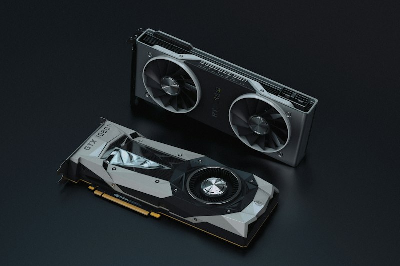
*Photo: China's AI compute strategy bets that system-level integration — more chips, better interconnects — can compensate for single-chip performance gaps. Image: Unsplash*
Challenges and Open Questions
None of this means Huawei has won. The challenges are substantial and, in some cases, structural.
Manufacturing capacity. SMIC's N+3 process — the 7nm-class technology underlying the Ascend 950DT — remains constrained. Huawei reportedly produces several hundred thousand Ascend chips per year, a fraction of what Nvidia ships. The 160,000-chip DeepSeek order alone would consume a significant share of annual output. Until SMIC ramps next-generation capacity or domestic EUV arrives, supply will remain the binding constraint.
Memory. CXMT, China's leading memory manufacturer, has begun producing small batches of HBM3E but remains three to five years behind Samsung, SK Hynix, and Micron, which are already mass-producing HBM4. Every Ascend chip needs HBM, and the HBM supply chain is almost entirely non-Chinese. This is the single most vulnerable point in the stack.
Software maturity. CANN has made enormous strides, and CANN-based clusters now run many of China's leading models. But CUDA's ecosystem — two decades of accumulated libraries, tools, developer expertise, and institutional knowledge — remains a moat that takes years to fill. The fact that Xing4.0 needed Day-0 adaptation by a third-party GPU vendor (MuXi) illustrates both the progress and the remaining fragmentation in China's software stack.
Single-chip gap. The Ascend 960DT's 2 PFLOPS of FP8 compute trails the Nvidia B300's estimated 4.5 PFLOPS by a wide margin. System architecture can compensate, but it cannot fully eliminate this gap, especially for workloads that do not parallelize well across thousands of chips. For training the largest frontier models, single-chip efficiency still matters enormously.
Export controls. The U.S. Bureau of Industry and Security's evolving restrictions on cloud-based remote access to AI chips — a rule reportedly taking effect in September — could limit how Chinese companies use overseas compute, while also restricting the reverse flow of expertise and services. The regulatory landscape remains volatile.
What This Means
The Ascend 960 SuperNode and the Wuhu 3D data center are not just product launches. They are the physical manifestation of a strategic pivot that China has been executing for seven years: from a model of technological convergence (buy the best chips, build on Western frameworks, compete on application) to one of technological divergence (build your own chips, write your own rules, compete on system architecture).
This pivot has implications that extend far beyond China's borders.
For Nvidia, the competitive threat is no longer hypothetical. Jensen Huang told CNBC in May that Nvidia had effectively "given up" the Chinese market to Huawei. The Ascend 960, with its NPO architecture and 4,096-chip supernode, is the most concrete evidence yet that Huawei is not merely filling a gap left by export controls — it is building infrastructure that Nvidia has not yet shipped.
For the global AI industry, the emergence of a genuinely parallel compute stack — different chips, different interconnects, different frameworks, different data center architectures — creates a bifurcation that will shape the next decade of AI development. Models trained on Ascend will be optimized for Ascend's strengths. Frameworks built on CANN will develop their own idioms and conventions. The AI world is not just splitting into American and Chinese camps politically; it is splitting technologically, at the level of silicon and photons.
For China specifically, the combination of system-level innovation (supernodes, NPO, 3D data centers) and manufacturing pragmatism (τ-law, mature-node chiplet stacking, vertical integration) offers a viable path to AI compute self-sufficiency. Not dominance — the single-chip gap and HBM dependency ensure that for the foreseeable future. But sufficiency, which is what Beijing actually needs. China does not need to beat Nvidia. It needs to ensure that no American policy decision can halt its AI development. The events of September 16-17, 2026, suggest that threshold has been crossed.
Huawei's roadmap makes the ambition explicit: Ascend 960DT ships in Q1 2027, three quarters ahead of schedule. The 960PR for inference follows in Q3 2027. The Ascend 970 arrives in 2028, the 980 in 2029 — a yearly cadence that mirrors Nvidia's. And He Tingbo's τ-law paper projects that by 2031, chips designed on time-scaling principles will achieve transistor density equivalent to today's 1.4nm process nodes.
The machine Wang Tao held aloft in Shanghai was small. The implications are not.
Social Media Reactions
@量子位 QbitAI (Weibo)
"4096颗芯片一台机器,华为把数据中心折叠成了一台超算。NPO近封装光学第一次量产商用,550千瓦功耗直接砍掉。这不是追赶,这是重新定义规则。(4,096 chips in one machine — Huawei folded a data center into a supercomputer. First mass-produced NPO, 550 kW power eliminated. This isn't catching up; it's redefining the rules.)"
@AI_jason (X/Twitter)
"Everyone's comparing Ascend 960DT to B300 on single-chip FLOPS and missing the point. It's a 4,096-chip *system*. The right comparison is GB300 NVL72 vs 960 SuperNode — and on system metrics, Huawei just took the lead on interconnect bandwidth and cluster scale."
@通信产业报 (WeChat)
"芜湖3D数据中心的意义不在技术炫技,而在工程效率。预制化装配把机电交付时间缩短一半,这意味着中国算力建设的瓶颈从'能不能建'变成了'芯片够不够'。供应链才是真正的战场。(Wuhu's significance isn't technical showmanship but engineering efficiency. Prefab cuts delivery time in half — the bottleneck shifts from construction to chip supply. The supply chain is the real battlefield.)"
@chipgirl_emily (X/Twitter)
"NPO is the story nobody's talking about. Nvidia announced co-packaged optics as a future roadmap item. Huawei is shipping it NOW, in volume, as the backbone of a 4K-chip supernode. They didn't just catch up on packaging — they lapped the field."
@半导体行业观察 (WeChat)
"中电信星辰4.0在纯国产算力上完成训练,这才是最重要的发布。硬件可以堆,生态必须养。当第一个10B+模型从昇腾训练出来且 benchmark 不输同类,CUDA 的护城河就开始松动了。(China Telecom's Xing4.0 trained on pure domestic compute — that is the most important release. Hardware can be stacked; ecosystems must be nurtured. When the first 10B+ model trained on Ascend matches benchmarks, CUDA's moat starts to crack.)"
@nathan_powell_ai (X/Twitter)
"The 2.75x MFU improvement for supernode-based 100K clusters vs traditional 8-GPU server clusters is the number that should terrify Nvidia. In a world where training runs cost $500M+, efficiency multipliers beat raw FLOPS. Huawei found the cheat code: stop selling chips, sell computers."
*Sources: Huawei Connect 2026 keynote presentations, China Daily, 36Kr, Jiuding Digital, Bloomberg, Pandaily, The Decoder, China Telecom announcements, ChinaXiv (He Tingbo, "A Time Scaling Theory for Multi-Layer Electronic Systems," May 2026), OIF technical documentation.*
Editor at AI in China. Tracking Chinese AI companies, funding rounds, and the technologies reshaping global tech. More about me.